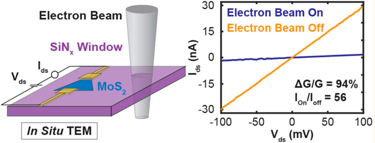
Researchers from the Drndić lab at the University of Pennsylvania used a Hummingbird Scientific in-situ TEM biasing holder to show a transmission electron microscope (TEM) field-effect transistor with electron beam gating. They used the electron beam to change the current−voltage characteristics of monolayer molybdenum disulfide (MoS2) channels on a silicon nitride substrate in-situ in the TEM. Using this technique, they show suppression of the conductance in the channel of up to 94%. Additionally, they report no structural damage to the MoS2 during gating, and the conductance changes back to its original value after the beam has been switched off. They published their findings in ACS Nano.

(Left) In-situ TEM device configuration: electron beam on a SiNx TEM window substrate containing a two-terminal MoS2 device. (Right) V-I characteristics of the transistor with the beam on and off. Copyright © 2020 American Chemical Society
Abstract: Paul Masih Das and Marija Drndić, In Situ 2D MoS2 Field-Effect Transistors with an Electron Beam Gate, ACS Nano 2020 Abstract
View All News

