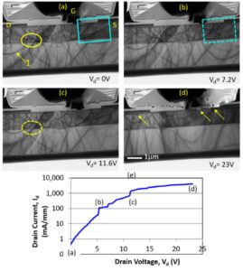
Researchers at Penn State University and Air Force Research Laboratory used one of the multiple types of Hummingbird Scientific in-situ TEM electrical biasing holders to study failure in GaN/AlGaN high electron mobility transistors. They used the removable sample carrier that provides a flexible platform to perform in-situ TEM biasing experiments to mount their transistor samples on a chip using FIB and visualize off-state failures. Through both TEM imaging, diffraction, and energy dispersive spectroscopy techniques, the researchers show that it is possible to use in-situ TEM to characterize the lattice defects and diffusion of various elements and correlate those to off-state failure modes.
They published their results in Applied Physics Letters.

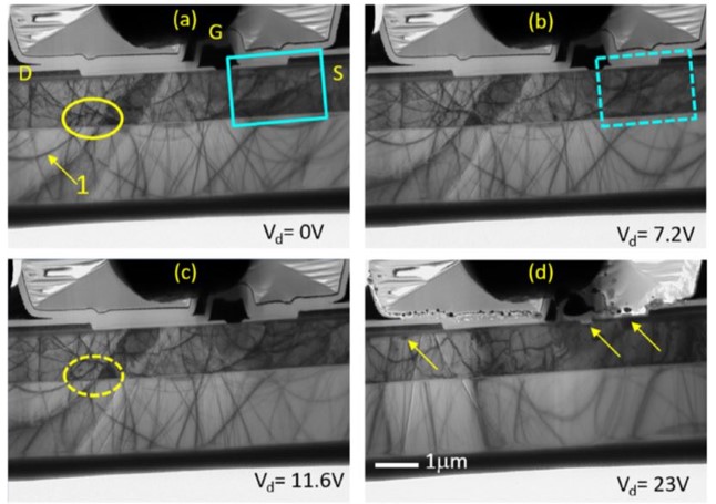
Bright field in-situ TEM images for a high electron mobility transistor specimen acquired at various drain voltages (a) at 0V; the oval and rectangular regions are identified to contain dislocations, while arrow 1 shows a bend contour (b) at 7.2V, (c) at 11.6V, and (d) at 23V; the three arrows indicate damage at the electrode interface. (e) Drain current vs. drain voltage data at gate voltage (5V), with the location of (a)–(d) labeled. Copyright (c) 2018 AIP Publishing
Reference: Zahabul Islam, Aman Haque, and Nicholas Glavin, Real-time visualization of GaN/AlGaN high electron mobility transistor failure at off-state, Appl. Phys. Lett. 113, 183102 (2018) Abstract
View All News

